http://britneyspears.ac/physics/pin/pn.htm
Consider a narrow band gap material of p-type semiconductor and a larger band gap material of N-type semiconductor are brought into contact. The Fermi level will be lined up to form an equilibrium state, in doing so the energy band will be bent, and a built-in electric field will be created between the junction. The modelling is similar to that of abrupt homojunction. I will not derive it again but just amend the previous derivation
Space charge distribution of p-N heterojunction:
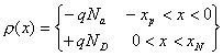
(1)
where N a and N D are the net ionized acceptor and donor concentration at p and N side, respectively. With Gauss's law, the electric field will be
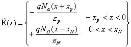
(2)
where ε p and ε N are the permittivity of p and N side, respectively. If we compare equation 2.26 with 2.9, we will find that the electric field is not continuous at x=0, but the normal displacement vector D =ε E is continuous at x =0; this will give you a same expression as
![]()
(3)
The electric field is a negative gradient of electrostatic potential, which means that the slope of the potential profile is given by the negative of the electric field profile. If we choose the reference potential to be zero for x < x p , we have
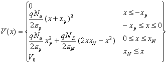
(4)
Again the contact potential is evaluated using the bulk values of the Fermi levels F p and F N measured from the valence or conduction band edges E vp and E CN, respectively, before contact, figure 5:
![]()
(5)
![]()
(6)
|
Figure 1. Bandedge profile before contact |
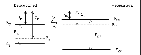
In figure 1,where Φ and χ are the work function that is the energy difference between the vacuum level and the Fermi level, and the electron affinity, which is the energy required to take an electron from the conduction band edge to the vacuum level.
The depletion length in the p side will be calculated once V 0 is known. Using equation 2.28 and 2.7, we have
![]()
(7)
and therefore
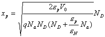
(8)
If the junction is under bias simply replaces V 0 to V 0 - V a
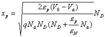
(9)
The energy band edge will be
![]()
(10)
![]()
(11)
(12)
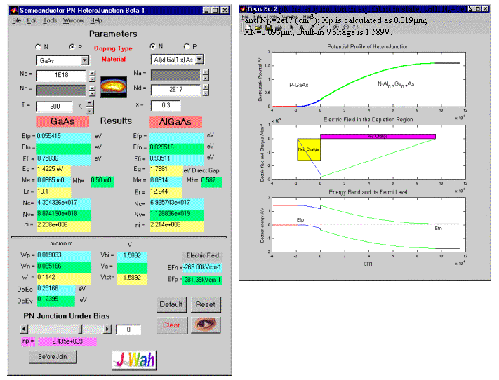
HeteroJunction Modelling
|
|
|
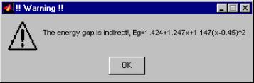
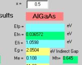
If you look at the electric field at x=0, you will find that the electric field is not continuous, simply because the permittivity of GaAs and Al x Ga 1-x As, are different between the two materials. However, the displacement vector is continuous at x=0. The space charge distribution is sketched in the second plot. In this control panel, the energy gap of AlGaAs was designed desirable in direct gap region, if the Al mole fraction was to excess 0.45 the system will indicate and warn you that you are using the indirect gap material that is not good for laser design.
This program also add-on an increment and decrement control on each concentration input. The radio buttons indicate that this is a p-GaAs and N-Al x Ga 1-x As Heterojunction. As usual the eye button is to call the program to plot potential profile, electric field, space charge distribution and energy band edges profiles.
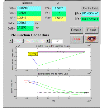
p-N Heterojunction Under Foward and Reverse Bias
 |
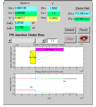 |
Figure 2: Reverse bias (-7V): X p =0.044mm, X n =0.221mm, V tot =8.5832V, electric field at x=0 –611kVcm -1
Forward bias(1.3V): X p =0.008mm,X n =0.0405mm, V tot =0.289V, electric field at x=0 –112kVcm -1

 留言列表
留言列表
